Electron Microscopy and Nanoengineering
Applied Materials Science, Department of Engineering Sciences, Uppsala University
Contact: Prof. Klaus Leifer
personal.teknik.uu.se/Teknikvetenskaper/elmin/
The group develops and applies high resolution electron microscopy techniques on atomic scale interfaces and nanomaterials. They also synthesise nanomaterials / -devices that derive their properties from interfaces, nanometer and subnanometer structures. The main techniques used and developed by this group are transmission electron microscopy, focussed ion beam and nanostructuring techniques used in the MSL laboratories. In these areas they also act as a competence resource for other MSL users, and all types of collaborations involving electron microscopy (TEM, SEM, FIB/SEM) and nanostructuring (FIB, E-beam lithography) are welcome.
Electron Microscopy
The group develops and refines techniques on quantitative high resolution electron microscopy (HRTEM, HRSEM) and spectroscopy techniques (EELS, EDS):
• Analysis of magnetic properties Electron Magnetic Circular Dichroism.
• Atomic resolution TEM using simulation for quantitative understanding of interfaces.
• Electron Energy Loss Spectroscopy and Cryo TEM for analysis of hard/soft matter interface in the TEM and FIB/SEM.
• 3-D electron tomography for nanoparticle analysis.
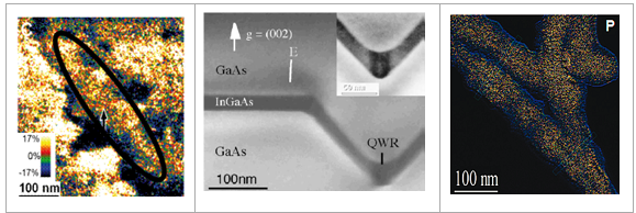
• Analysis of local structure, strain and chemical composition in quantum dots and quantum wires.
• Quantitative TEM analysis of amorphous materials.

EMCD map of the magnetisation in an Fe map. The marked region shows an EMCD signal with a sub-nanometer resolution (left). Quantitative strain imaging of quantum wires (middle). Chemical mapping of distribution of DNA (right).
Nanoengineering for Materials Property Analysis and Sensing
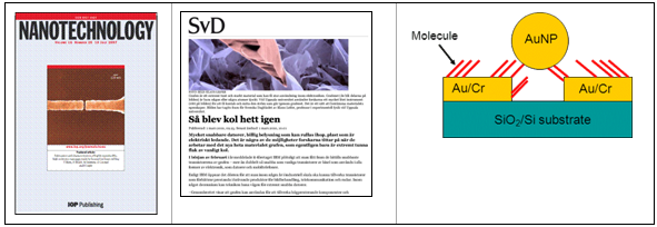
The group develops nanostructuring fabrication schemes to analyse fundamental properties of nanoparticles, rods, molecules and 2-D materials such as graphene. Photolithography, electron beam lithography and FIB techniques are used for micro- and nanostructuring. These devices are developed into sensing devices for gases and bio-molecules.

Development of ultra-high resistance nano-electrodes for assessment of electrical properties of nanoparticles and single molecules (left). Nanomanipulator touching an individual graphene sheet (middle). Nanoelectrode-molecule-nanoparticle bridge platform for assessing electrical properties of down to single molecules (right).